 Laplace Deep Level Transient Spectroscopy is used to study
electrically active impurities and defects in semiconductors. It has a higher
sensitivity than almost any other technique (in 20 Ohmcm
silicon it can detect impurities at a concentration of one part in a million million) and has sufficiently high energy resolution (a few
meV) to reveal information on the impurity’s local
environment such as stress or atomic siting. The invention of the experimental technique of Laplace DLTS
was awarded the
Laplace Deep Level Transient Spectroscopy is used to study
electrically active impurities and defects in semiconductors. It has a higher
sensitivity than almost any other technique (in 20 Ohmcm
silicon it can detect impurities at a concentration of one part in a million million) and has sufficiently high energy resolution (a few
meV) to reveal information on the impurity’s local
environment such as stress or atomic siting. The invention of the experimental technique of Laplace DLTS
was awarded the
 The experimental
techniques were developed at the Institute of Physics Polish Academy of
Sciences in
The experimental
techniques were developed at the Institute of Physics Polish Academy of
Sciences in
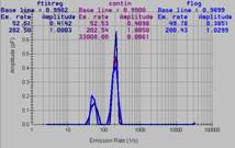
 At the
heart of the method are mathematical routines which convert the recorded
relaxation process (measured as a capacitance or current transient) from the
time domain into a spectrum of time constants (in the case shown electron
emission rates) in the frequency domain.
At the
heart of the method are mathematical routines which convert the recorded
relaxation process (measured as a capacitance or current transient) from the
time domain into a spectrum of time constants (in the case shown electron
emission rates) in the frequency domain.
The implementation of Laplace Deep Level Spectroscopy increases the
energy resolution of conventional DLTS by an order of magnitude and makes it
possible to observe effects and processes which are impossible to see with the
usual methods. Two examples are shown below but go to the pages on Key Results and
on LDLTS Literature sections for more
details.
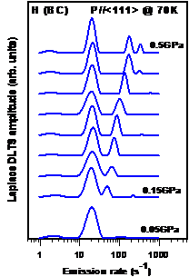
 On the left-hand side. Uniaxial stress induced splitting of the
Laplace DLTS peak related to the bond-centred hydrogen in silicon is shown. The
splitting pattern indicates the trigonal symmetry of
the defect.. Phys. Rev. B, 65, 075205, (2002), PDF (90kB)
On the left-hand side. Uniaxial stress induced splitting of the
Laplace DLTS peak related to the bond-centred hydrogen in silicon is shown. The
splitting pattern indicates the trigonal symmetry of
the defect.. Phys. Rev. B, 65, 075205, (2002), PDF (90kB)
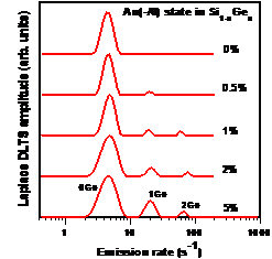
On the right-hand side. The appearance of the alloy splitting pattern observed for the gold
acceptor state in silicon-germanium alloys. Phys. Rev. Lett., 83, 4582 (1999);
Phys. Rev. B, 63, 235309 (2001)