Key Results (still under construction)
A review of scientific results obtained
with a use of the Laplace DLTS method is given in the review paper [J. Appl.
Phys., 96, 4689 (2004); PDF (900kB)]
or in scientific papers listed in the Literature section.
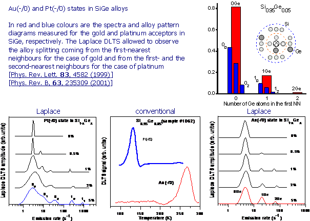
Alloy splitting of the defect
electronic level
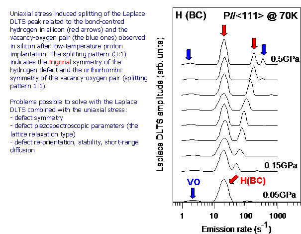
Laplace DLTS combined with uniaxial stress technique
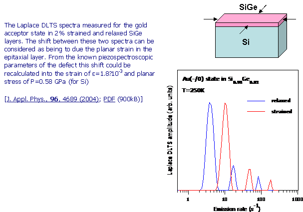
Probing the epitaxial layer strain
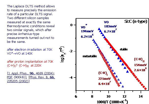
Arrhenius-plot for defect
identification/testing
Energy-state distribution of the Pb centers at the Si/SiO2 interface
Alloy splitting of the defect electronic
level
[Top]
[Top]
Probing the epitaxial
layer strain
[Top]
Arrhenius-plot for defect
identification/testing
[Top]
Energy-state distributions of the Pb
centers at the (100), (110), and (111) Si/SiO2 interfaces
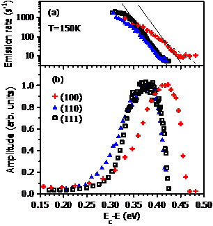 The energy distribution of the Pb
centers at the (100), (110), and (111) the Si/SiO2 interface has
been determined. For the (111) and (110) interface orientations the
distributions are similar and centered at 0.38eV below the silicon conduction
band. This is consistent with only Pb0 states being present. For the
(100) orientation two types of the interface states are observed; one similar
to the (111) and (110) orientations while the other has a negative-U character
in which the emission rate versus surface potential dependence is qualitatively
different from that observed for Pb0 and is presumed to be Pb1.
The energy distribution of the Pb
centers at the (100), (110), and (111) the Si/SiO2 interface has
been determined. For the (111) and (110) interface orientations the
distributions are similar and centered at 0.38eV below the silicon conduction
band. This is consistent with only Pb0 states being present. For the
(100) orientation two types of the interface states are observed; one similar
to the (111) and (110) orientations while the other has a negative-U character
in which the emission rate versus surface potential dependence is qualitatively
different from that observed for Pb0 and is presumed to be Pb1.
The figure shows the emission rates (a) and
normalized DLTS signal amplitudes (b) observed for the Pb
states at the Si/SiO2 interface with different orientations. The
energy on the horizontal axis is the difference between the bottom of the
conduction band and the Fermi level cross-point at the interface. The solid
lines slope in (a) is 1/(kBT)
(T=150K), while for the dashed line is 1/(2kBT). See the Applied Physics Letters 92,
242104 (2008) article for more details.
[Top]