Laplace Deep Level Transient Spectroscopy is used to study electrically active impurities and defects in semiconductors. It has a higher sensitivity than almost any other technique (in 20 Ohm-cm silicon it can detect impurities at a concentration of one part in a million million) and has sufficiently high energy resolution (a few meV) to reveal information on the impurity’s local environment such as stress or atomic siting. These Web pages explain how the technique works, provide links to some of the scientific results obtained and give guidance if you want to set up the technique in your own laboratory including software downloads. In addition you can access our database of DLTS and Laplace DLTS results and enter your own data into our on-line calculator to compare with defect signatures in the database.
In 1993 L. Dobaczewski, I. D. Hawkins and A. R. Peaker were awarded the UK
National Physical Laboratory (http://www NULL.npl NULL.co NULL.uk/) prize for the invention of Laplace DLTS this was followed by a Royal Academy of Engineering Foresight Award in 1997. Laplace DLTS was subsequently developed within several scientific
projects funded by the European Union, the Polish Ministry of Science and Higher Education and the
Foundation for Polish Science (http://www NULL.fnp NULL.org NULL.pl/ang/index NULL.html) in Poland, and by the
Engineering and Physical Sciences Research Council (http://gow NULL.epsrc NULL.ac NULL.uk/ViewGrant NULL.aspx?GrantRef=EP/C009738/1) in the United Kingdom.
The software and hardware were developed at the Institute of Physics Polish Academy of Sciences in Warsaw and at the Microelectronics and Nanostructure Group, School of Electrical and Electronic Engineering at the University of Manchester. Work is now in progress at the Institute of Physics (http://www NULL.ifpan NULL.edu NULL.pl/index_en NULL.php) in Warsaw and the Photon Science Institute (http://www NULL.psi NULL.manchester NULL.ac NULL.uk/) at the University of Manchester on an optically excited version of Laplace DLTS for wide band gap semiconductors. We are also working with a number of collaborators to apply the Laplace hardware and software we have developed to other branches of science.


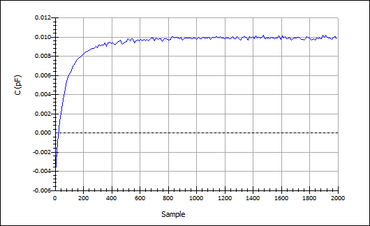
At the heart of the method are mathematical routines which convert the defect relaxation process (measured e.g. as a current or capacitance transient, as shown on the left) from the time domain into a spectrum of time constants (in the case shown electron emission rates) in the frequency domain. Laplace Deep Level Spectroscopy provides an increase in energy resolution over conventional DLTS of an order of magnitude. This makes it possible to observe effects and processes which are impossible to see with the usual methods.
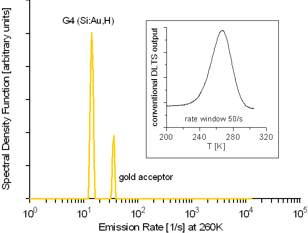
The example on the right shows the case of gold in silicon. The inset DLTS plot shows one peak with very slight broadening. The main plot shows a measurement of the same sample using Laplace DLTS. It is clearly evident there are two distinct defects, one of these is due to substitutional gold the other to a gold hydrogen complex.
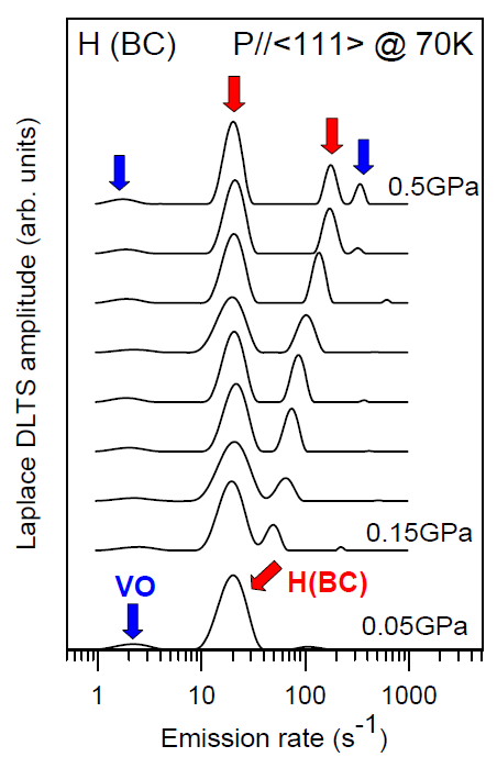
Uniaxial stress induced splitting of the Laplace DLTS peak related to the bond-centred hydrogen in silicon is shown. The splitting pattern indicates the trigonal symmetry of the defect.
Phys. Rev. B, 65, 075205, (2002) (http://dx NULL.doi NULL.org/10 NULL.1103/PhysRevB NULL.65 NULL.075205),
PDF (90kB)

Appearance of the alloy splitting pattern observed for the gold acceptor state in silicon-germanium alloys.
Phys. Rev. Lett., 83, 4582 (1999) (http://dx NULL.doi NULL.org/10 NULL.1103/PhysRevLett NULL.83 NULL.4582);
Phys. Rev. B, 63, 235309 (2001) (http://dx NULL.doi NULL.org/10 NULL.1103/PhysRevB NULL.63 NULL.235309)
 Appearance of the alloy splitting pattern observed for the gold acceptor state in silicon-germanium alloys. Phys. Rev. Lett., 83, 4582 (1999) (http://dx NULL.doi NULL.org/10 NULL.1103/PhysRevLett NULL.83 NULL.4582); Phys. Rev. B, 63, 235309 (2001) (http://dx NULL.doi NULL.org/10 NULL.1103/PhysRevB NULL.63 NULL.235309)